Quick Review of Flex Design Options
- Static: Not meant to flex
- Flex to Install: Only meant to flex on limited basis. To install or replace
- Dynamic: Depending on flex construction and conditions this could result in >1M flex cycles
- Back Bared Pads / Back Side Access – This is a flex that is typically single sided in construction but has the copper accessed from both sides.
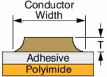
- Conductor aspect ratio – Relationship of conductor width to conductor height. General rule of thumb is conductor width should be greater then 5 times the conductor thickness.
- Coverfilm / Coverlay -This is the insulating material, usually in a film format, that is laminated to the flex circuit to define solderable areas. Can be drilled, laser cut or chemically removed to create complex geometries.
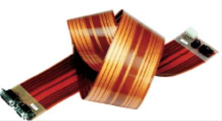
- Dynamic –A type of flexible circuit that will see repeated flexing, sometimes more than 1 million cycles, such as in a disk drive, mobile phone or laptop computer.
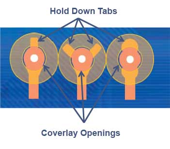
- Hold Down Tabs -These are extensions of the copper pad and are used to help anchor the pad during soldering processes both in assembly and rework.
- I-Beam Effect -This is the result of stacking your conductors during your design. Subsequent flexing induces stress and compression, causing cracking to occur.
- PIC, Photoimagable Coverfilm / Coverlay -This is another means of defining your solderable areas. This material is apply in a clean room environment, exposed with an artwork and then developed. This allows for complex geometries not available from routing or other soft tooling means.
- PSA (Pressure Sensitive Adhesive) -An adhesive used to bond stiffeners to specific regions of the flex circuit
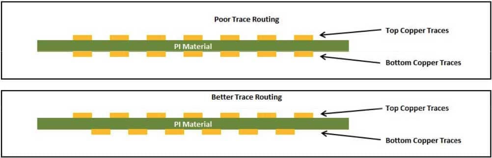
Always try to avoid “stacking traces” in the same location from layer to layer.
Hold Down Tabs/Pad Staking
Stress from bending/flexing can cause issues with the copper pads maintaining adhesion to the base material. The addition of copper extending under the coverlay will help maintain the adhesion of the pads.
Calculating Minimum Bend Radius
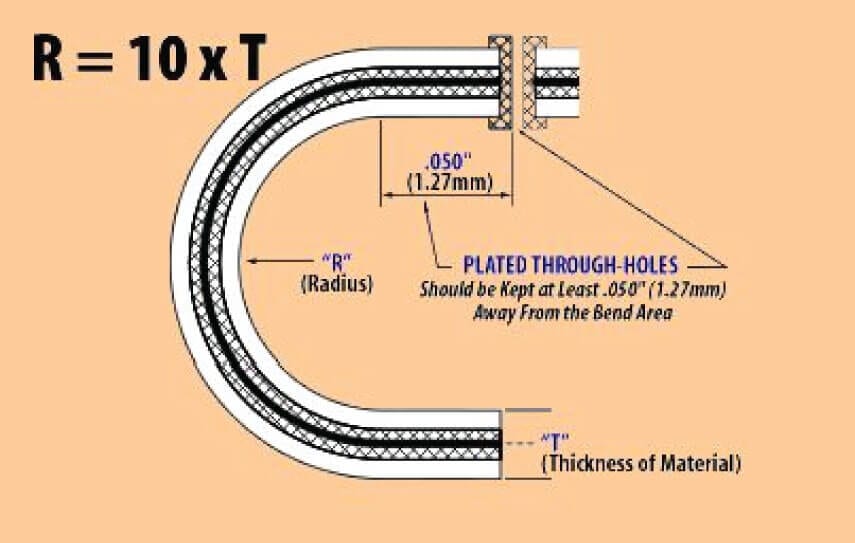
The general guideline for calculating minimum bend radius is 10X the total thickness of the flexible circuit for double sided (2 layer) applications.
The general guideline for calculating minimum bend radius is 6X the total thickness of the flexible circuit for single sided (1 layer) applications.
The general guideline for calculating minimum bend radius is 20X -25X the total thickness of the flexible circuit for multi-layer (3+ layers) applications.
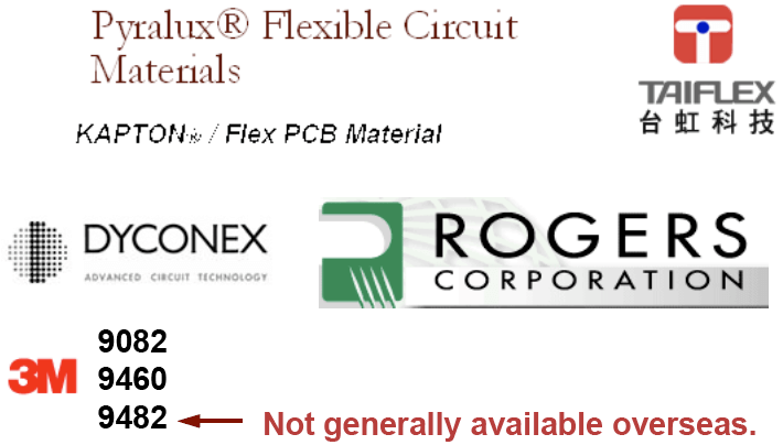
PCB Solutions recommends Taiflex material for most flexible applications, due to cost, performance and lead-time overseas.