Radio Frequency (RF) & Microwave Printed Circuit Board Capabilities
In addition to rigid, flex, rigid-flex and aluminum circuit board production, PCB Solutions offers strong engineering and manufacturing support for Radio Frequency (RF) and Microwave PCBs. As the world electronics field is ever expanding into products that move at faster speeds with mixed signal technology, the need for more complex circuit production has never been more important.
PCB Solutions has years of RF and and Microwave engineering and manufacturing experience. Here is a summary of our technology stack and experience:
- Quick Turn / Prototype / Production
- Mixed FR-4 Material / PTFE Laminates:
- Rogers ML, AD, CLTE, CuClad, DiClad, ISOClad, KAPPA, MAGTREX, XtremeSpeed RO2100, RO3000, RO4000, RT/DUROID 5000 (5880), RT/DUROID 6000, TC, and TMM Series
- Rogers Bonding Materials
- EMC material including: EM-39B prepreg / EMC EM390 cores
- V-Tec, Isola, Dupont, Nelco, Tactonic, Arlon
- Sequential Lamination
- Drilling
- Minimum Drill – .0059”
- Standard Drill – .010”
- Controlled Depth Routing & Laser Drilling
- Blind / Buried Vias. & Micro Vias
- Via In Pad
- Controlled Impedance
- Max Panel Size 24” x 30”
- Unique Copper Weight
- ¼ oz, no plating
- ½ oz, no plating
- Tolerances
- Outerlayer Trace / Space .003” / .004”
- Innerlayer Trace / Space .003 / .004”
- 15:1 Aspect Ratio
- Surface Finish Considerations
- Nickel
- ENIG
- OSP
- Via Plugging
- Conductive
- Non-conductive
- Copper Plug
In addition to solid engineering and manufacturing, our volume purchasing power for high tech materials gives a competitive advantage for offering much lower cost RF and Microwave PCB production.
With a complex manufacturing process for high speed and mixed signal electronics, we have created an overview from a Design For Manufacturing engineer’s point of view. You can view this in-depth overview of RF and Microwave designs below.
Radio Frequency and Microwave PCB Overview
Overview:
With the rapid increase of IoT (Internet of Things) sensors, smartphones, wireless electronics and 5G, the electronics manufacturing world is seeing a corresponding increase RF and Microwave printed circuit board production.
With the complexities of RF printed circuit design and manufacturing, PCB Solutions can assist in the design, engineering, bare board manufacturing and assembly of these challenging products.
The Printed Circuit industry considers any high frequency PCB operating at 100 MHz an RF (Radio Frequency) product. Within the RF class, any product operating at or above 2GHz is considered a Microwave printed circuit board.
RF and Microwave printed circuits present unique challenges in both design and manufacturing due to problems that may arise within the signals when transmitting and receiving the radio signals. These concerns may not only be macro level issues such as the overall signal transmission and strength, but micro issues such as signal noise, cross talk, signal loss and thermal interference.
To combat these issues RF and Microwave designs typically incorporate much tighter and more complex impedance constraints, specific trace routing techniques, advanced materials and more. We will expand on each of these considerations below.
RF and Microwave Printed Circuit Board Materials:
Materials used in RF and Microwave Printed Circuit applications are typically some combination of PTFE, ceramics, hydrocarbon, and various forms of epoxy/woven glass. These materials usually have very specific characteristics for dielectric constant (Er), loss tangent, and co-efficient of thermal expansion (CTE).
High frequency circuit materials with a low stable dielectric constant and low loss tangent allow for higher speed signals to travel throughout the printed circuit board with less impedance than standard FR-4 printed circuit board materials. It is possible to mix these materials in the same stack-up to achieve optimal performance and cost effectiveness.
Advantages of using specific RF or microwave materials designed for high frequencies include:
- Material will remain very stable in high temperature environments while operating at very high frequencies.
- Material will allow for the effective placement of very fine pitch components including high I/O Ball Grid Arrays, large QFN’s and QFP’s and even bare die-attach, which are all common in large scale communication assemblies.
- Allow for dense routing and specific impedance-controlled traces as well as the alignment of multiple layers and the specific features often present in a complex high frequency printed circuit designs.
PTFE (polytetrafluoroethylene) with micro-glass fiber or woven glass is the most common material used in high frequency Printed Circuit Boards. This material typically consists of a synthetic thermoplastic fluoropolymer. PTFE material will come at a premium cost; however many engineers believe the PTFE attributes of consistent dielectric properties, low CTE (coefficient of thermal expansion) and excellent thermal conductivity make this the desired RF and Microwave material, despite its typically higher price. For those on tighter budgets, ceramic filled PTFE may fulfill the desired requirements at a lower price.
There are several factors and material properties to consider when choosing your high frequency material, some of which we will detail below. It is highly recommended to consult with your electrical engineering staff and closely read material data sheets to find the best material match for your application.
Coefficient of thermal expansion (CTE)
- The coefficient of thermal expansion (CTE) is a direct relation of how an object’s size varies with a change in temperature. It is also a way to measure the thermal robustness of the material. The CTE of a material will have a direct impact on several critical steps in the printed circuit manufacturing process including primary drilling, lamination as well as the often thermally challenging assembly stages of high frequency printed circuit boards.
- In a multilayer high frequency or microwave printed circuit stack-ups, the use of different materials with varying CTE’s will directly affect the features at different rates. This effect can cause feature alignment issues, via annular ring breakout and impedance issues.
- During component assembly, the CTE has a direct affect on both reflow and wave soldering. The CTE will have a direct correlation to how well the assembly handles the various thermal cycles required for advanced assembly. A material with poor CTE can lead to cracked boards, insufficient pad wetting, poor solderability, and in severe cases cracked printed circuit boards and damaged components. To mitigate these potential issues a material with a low CTE should be chosen.
Dielectric Constant
- Controlling impedance and impedance matching is critical with high frequency boards. As RF and microwave frequencies move higher, the acceptable impedance tolerances become smaller. Typically, specific signals in your printed circuit need to be matched, for instance your driver signal may need to be 50 ohms, not only from the driver, but during transmission and to the receiver as well.
- Traditional FR4 printed circuits may be able to utilize a single set of impedance values including dielectric constants, copper thicknesses and dielectric distances. However, RF and microwave designs often need to mix these critical variables to better control the specific impedance needs of the high frequency design.
- The dielectric constant measures a material’s ability to store electrical energy in an electric field. This value is typically direction-dependent, so the dielectric constant may change or fluctuate depending on the axis of the material. This means it is possible the dielectric constant may can shift under the high frequency conditions of RF or microwave applications, so it is important to understand what frequency range the material was tested under, what testing method was used and if there are values available for frequency ranges and conditions that closely match your target application. This information is supplied by the material vendor and is typically found in the data sheet.
Loss Tangent:
- A material’s loss tangent gives a measure of power lost due to the material. The lower a material’s loss tangent, the less power lost. The loss tangent of most FR4 materials range from 0.02 for most commonly used materials to 0.001 for very low-loss high-end material typically used in high frequency applications.
- All PCB materials have both conduction losses and dielectric losses. The conduction losses are resistive and are caused by the conductive copper layer used in the board. The dielectric losses on the other hand are associated with the substrate (insulating material) used in a PCB. When the electric field is applied, polarization can occur, and charges are displaced relative to the electric field. Dielectric losses cause a reduction in the overall electric field. The total amount of polarization that can occur in a dielectric depends upon the molecular symmetry of the insulator material and is called Dipole Moment. The effect of the dipole moment in a dielectric substrate is termed Loss Tangent.
- The signal loss by the dielectric material depends upon the material’s structure and composition. Selection of low loss materials is the major task for manufacturers that is why they are advised to plot the attenuation equation against frequency for various material choices.
- Loss tangent plays a crucial factor for very high frequencies above 1 GHz and analog signals to determine the signal attenuation. Therefore, the selection of low CTE, or Low-loss material is critical in these applications.
RF and Microwave Design:
High frequency designs often require specialized set of criteria to offset the challenges associated with the stronger electromagnetic field and effects which naturally occur at these higher frequencies. These fields can induce signals in adjacent copper features or PCB traces, creating undesirable crosstalk (interference and overall noise) which may undermine system performance. Return loss (signals reflected back into the adjacent oncoming signal) is primarily caused by impedance mismatches and may create much of the same impact of added noise and interference to the primary signal.
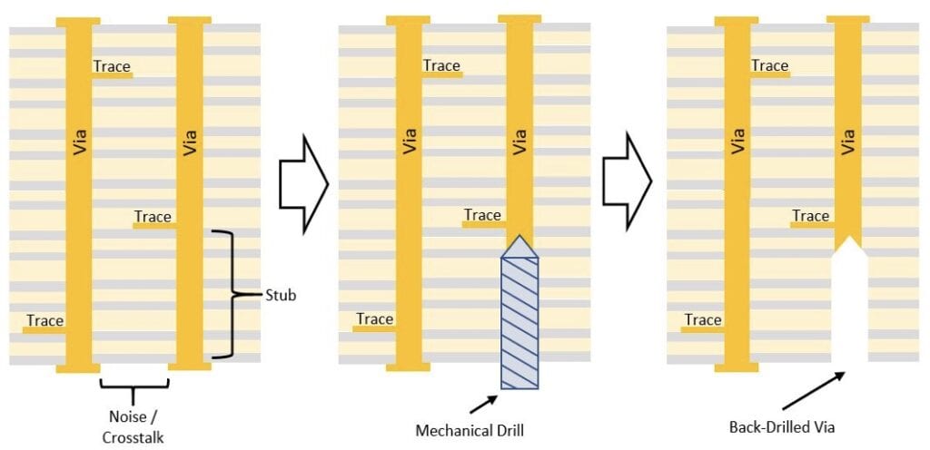
The primary way to manage unwanted crosstalk is by ground plane management, trace-to-trace spacing, and/or reduction of stubs either through design or the use of depth-controlled back drilling.
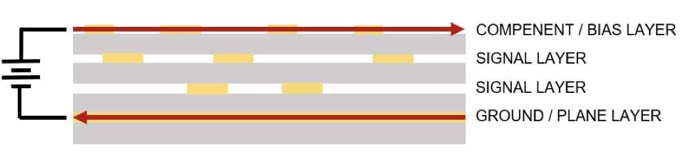
- The return current path for system bias layers typically needs to be considered in an RF design. Adding signal layers between a bias and ground layer will create a larger return path as shown below, resulting in noise coupling on the signal layers. It is recommended to ensure there are not any signal layers between your bias and ground return layers.
- Feature or copper spacing are critical in RF applications, due to crosstalk and something referred to as the “skin effect.” When the “skin effect” occurs, the effective resistance of the copper traces on your board will increase due to a reduction in the available cross-sectional area for current flow. This effect manifest itself when the resistance of a trace begins to increase, leading to resistive losses, as well as adding heat to the circuit. Care must be taken in feature and specifically trace to trace spacing to mitigate this effect on the design and functionality of the printed circuit board.
- Crosstalk or signal noise is when the board features or signals begin interacting with itself, such as signals bleeding over into nearby components and undesired coupling. Another definition of crosstalk is the unintentional electromagnetic coupling between traces on a printed circuit board. The overpowering of one signal in a trace by another one is the result of this coupling even though the two traces are not in physical contact with each other. In addition to potential for crosstalk between two traces that are side-by-side on the same layer, there is an even greater risk for traces that are running parallel to each other vertically between two layers. This effect is known as broadside coupling and happens when the two signal layers are separated by only a very small dielectric distance of core material. This dielectric distance is often less than the spacing between two traces on the same layer. Options to mitigate the risks of crosstalk or signal noise are outlines below:
- Layout signal layers on your board layers so that two adjacent signal layers (example layers two and three) will have preferred routing directions that cross each other instead of running parallel to each other. If layer two is running “top to bottom,” then make sure that layer three is running “right to left.” This layout technique can minimize the possibility of broadside coupling.
- Use ground planes between two adjacent signal layers to further reduce the potential for broadside coupling. This will not only increase the distance between the layers but also this configuration may also provide a more efficient return path through the ground plane. Be cautious of the bias layer and return path plane layer as described above when utilizing this strategy.
- Ensure adequate space from high speed routing such as differential pairs and clock signals to other circuits. A general guideline is to space out traces at three times their nominal line width when measured center to center. It is estimated this can reduce the electrical interference by as much as 70%.
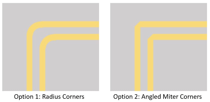
- The addition of line bends and corner compensation will aid in impedance control if your transmission lines need to change direction. A typical bend radius that is at least 3 times the center conductor width is preferred. This will ensure that impedance remains consistent as current travels through the bend as your transition line changes direction. If your design tool does not allow a gentle radius, or other factors prevent you from doing so, then it is recommended to use an angled miter corner as shown below. This will greatly help to reduce impedance fluctuations.
Backdrilling, or controlled depth drilling, is the process of removing the conductive plating in vias. The unused portion of the via that serves no functional purpose to the circuit is called a stub. In high frequency RF or Microwave circuit designs, these stubs can become a significant source of signal noise, cross talk, and signal distortion. The back drilling process is achieved by performing a secondary drill process after the vias have been plated using a drill bit slightly larger than the via itself at a controlled depth, typically about .010” from the last used inner layer signal connection.
PCB Solutions advanced RF and Microwave Capabilities:
- Up to 30 Layers
- Up to 20:1 Plated Hole Aspect Ratio
- Advanced Materials (Isola, Rogers, Arlon, Taconic, Panasonic Megtron)
- Blind, Buried, and micro vias including ELIC (Every Layer Interconnect), Stacked Micro vias, and via-in-pad
- .006” mechanical via holes
- .003” trace with and spacing for both inner and outer layers
- .002” minimum dielectric distances
- Controlled depth drilling, controlled depth routing and back drilling
Summary:
Finding a capable RF and Microwave printed circuit manufacturer is critical to ensuring the products will have the optimal design, material and engineering required to supply a high functioning and reliable product to the market. PCB Solutions robust network of domestic and offshore manufacturing partners will prove to be one of your most valuable assets in delivering quality, on time and competitively priced product to your end users.
Start Your Quote
Call 801-361-1228Companies We Serve