Printed Circuit Assembly, also known as Printed Circuit Board Assembly (PCBA), is the process of creating a final assembled and functional electronic assembly by populating and soldering electronic components onto a bare printed circuit board (PCB).
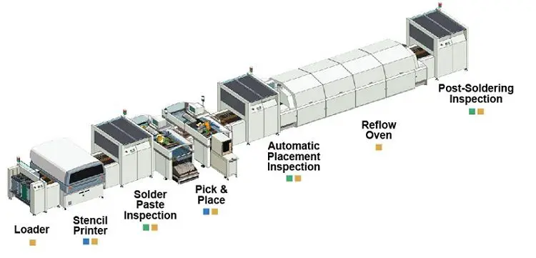
The process of printed circuit assembly typically involves the following steps:
Bare Printed Circuit Board (PCB) Fabrication
The first step is to manufacture the unpopulated Printed Circuit Board itself. It involves designing the circuit layout using various Electronic Design Automation (EDA) tools including Schematic Capture, Electronic Computer Aided Design (ECAD), automatic component placement and circuit routing tools and other specialized software. When the design is completed, the bare PCB will be fabricated by etching copper traces on a non-conductive substrate, such as fiberglass or epoxy. There are many advanced technologies used during both the design and fabrication of the bare printed circuit board.
Solder Paste Application and Inspection
Solder paste is a key material used in printed circuit board assemblies. It is a mixture of powdered solder alloy and flux, combined to form a homogenous paste-like consistency. The primary purpose of solder paste is to hold the surface mount components in place and facilitate the soldering process of the PCB assembly during the reflow component assembly process.
Solder paste typically consists of three main components: solder powder, flux, and a binder. The solder powder is made up of a specific alloy, commonly lead-free compositions like tin-silver-copper (Sn-Ag-Cu) or tin-bismuth (Sn-Bi). The flux is a chemical compound that helps clean the metal surfaces, prevent oxidation, and promote the proper wetting and flow of solder in the reflow oven during the reflow component assembly process. The binder holds the solder particles and flux together in a stable paste form.
Solder pastes can contain different types of flux, such as rosin-based or water-soluble flux. Rosin-based fluxes are composed of natural or synthetic resins and are often used in traditional soldering applications. Water-soluble fluxes offer easier post-solder cleaning. The choice of flux depends on the specific requirements of the PCB assembly process and the subsequent cleaning methods.
The size of the solder particles in the paste has a significant impact on the soldering process. The particle size distribution is typically specified by the solder paste manufacturer. Finer particles enable precise deposition, especially for small components and fine-pitch circuitry, while larger particles are suitable for larger components and high-thermal-mass applications.
Solder paste is applied to the PCB using a stencil or a dispenser. Stencils are commonly used for mass production, where the paste is spread over the stencil and forced through the apertures onto the PCB pads using a squeegee. Dispensers, on the other hand, are used for selective soldering, where the paste is precisely deposited onto specific areas or components prior to placement on the printed circuit board.
Solder paste is a sensitive material that requires proper storage and handling. It is typically stored in a controlled environment, such as a refrigerator, to prevent oxidation and maintain its consistency. The solder paste will need to be allowed to reach room temperature prior to use to avoid issues with viscosity and soldering performance.
It’s important to note that solder paste formulations and application techniques can vary depending on specific requirements, such as lead-free vs. leaded soldering, environmental regulations, and the specific characteristics of the PCB assembly. Manufacturers often provide detailed instructions and datasheets with specific recommendations for their solder paste products.
Solder paste is typically inspected after application. Solder paste inspection (SPI) is a critical step in the component assembly process. It involves inspecting the application of solder paste onto printed circuit boards prior to the components being placed and soldered. The purpose of Solder Paste Inspection is to ensure the quality and accuracy of the solder paste deposition, which directly affects the overall solder joint reliability and the performance of the electronic assemblies.
SPI is performed using specialized inspection machines called solder paste inspection systems. These machines consist of a high-resolution camera, lighting system, image processing algorithms, and software for analysis and reporting. The inspection system captures high-resolution images of the PCB’s solder paste deposits. The captured images are processed by advanced algorithms to identify and measure various attributes of the solder paste deposits including the solder paste volume, area, height, shape, and position.
The measured data is compared against predefined specifications and tolerances to determine the acceptability of the solder paste deposits. The SPI system identifies various defects in the solder paste application, such as insufficient or excessive solder paste volume, bridging of solder paste between surface mount pads, misalignment, or missing solder paste. The SPI system generates detailed reports summarizing the inspection results, including statistical data, images, and defect classifications. This information is valuable for process optimization, yield improvement, quality control, and traceability.
Component Placement
Once the PCB fabrication is complete, electronic components such as resistors, capacitors, integrated circuits (ICs), connectors, and other active and passive components are placed on the board. This process can be done manually or using automated pick-and-place machines, depending on the scale of production.
The pick and place process involves the precise and efficient handling of small electronic components, such as resistors, capacitors, integrated circuits (ICs), and other surface-mount devices, as well as, through hole-leaded parts such as connectors. Traditionally, this task was performed manually by skilled operators, but with the advancement of surface mount placement technology, automated pick and place machines have become the industry standard due to their speed, accuracy, and cost-effectiveness.
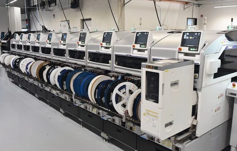
The automated component placement machines typically consist of the following elements:
- Component Feeding: The machine is equipped with multiple component feeders containing different electronic components. These feeders are loaded with reels or trays that hold the components securely allowing specific electronic components to be selected for placement at the appropriate time.
- Vision System: Most modern pick and place machines have a vision system composed of cameras and sensors. These systems help in identifying the components selected from the feeders and verifying the correct components are selected, as well as the components orientation, and accurate placement. The vision systems can use images and shapes from a centralized library, or use known good parts in the assembly as references.
- Component Pickup: Assembly pick and place machines typically utilize a vacuum nozzle or a mechanical gripper to pick up components from the feeders and place them on the printed circuit board prior to soldering. The nozzle applies suction to hold the component firmly while it is being transported and placed in the correct location on the bare printed circuit board.
- Placement: The pick and place machine precisely moves the component to the target location on the printed circuit board and places them. Vision systems help align the component with the correct orientation and ensure accurate placement. This placement may involve rotating components and making fine adjustments based on the vision system.
Advantages of automatic electronic pick and place machines:
- Speed and Efficiency: These machines can place components at a significantly faster rate compared to manual labor, resulting in higher production output. Multiple component pick and place machines may be utilized in series or parallel to increase production capabilities.
- Accuracy and Precision: Automated pick and place machines offer exceptional accuracy, ensuring precise component placement, which is crucial for proper circuit functioning and allow for closer component spacing which maximizes the usable area of the printed circuit assembly.
- Consistency: The machines maintain consistent quality across multiple production runs, reducing the risk of human error and ensuring product reliability.
- Cost-Effectiveness: While the initial investment in pick and place machines as well as the multiple component feeders can be high, the long-term benefits, such as increased production capacity, higher yields, increased quality and reduced labor costs, make them cost-effective in high-volume manufacturing environments.
- Flexibility: Modern pick and place machines are often equipped with multiple heads and can handle a wide range of component sizes, shapes, and types, offering versatility in production. Component pick and place machines may be set up for large production runs, or flexibility in high mix prototyping environments.
Automatic electronic pick and place machines have revolutionized the electronics manufacturing industry by automating a critical and labor-intensive process. They improve efficiency, quality, and productivity while reducing manufacturing costs, making them indispensable tools in modern electronics assembly lines.
Soldering
After placement, the printed circuit board with the electrical components placed moves to the soldering process. Several different processes can be used to permanently solder the components to the printed circuit board including:
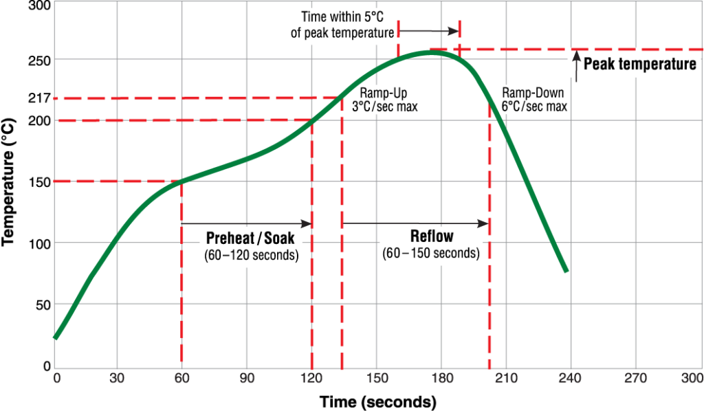
- Reflow Soldering: After the solder paste is applied to the PCB, the assembly undergoes a reflow soldering process. During reflow, the PCB is heated in a controlled manner, typically a solder reflow oven, to melt the solder paste, allowing it to bond with the component leads and printed circuit pads. The flux in the solder paste helps remove any oxidation and contaminants, ensuring a reliable solder joint. The printed circuit board, together with the solder paste and components is typically preheated before entering the reflow oven. Preheating eliminates moisture and prepares the board for the reflow soldering process.
The PCB is transported through a reflow oven on a conveyor belt. The reflow oven has different zones, each with specific temperature profiles. These zones include preheat, soak, reflow, and cooling zones. Each zone as well as the temperature ramp up and down, time spent at temperature and speed of the assembly through the reflow oven can be unique and is referred to as the reflow profile for the particular assembly.
- Preheat Zone: In this zone, the PCB is gradually heated to a temperature that evaporates any remaining moisture and activates the flux in the solder paste. The flux helps remove oxidation from the metal surfaces, ensuring good solder wetting and reliable solder joints.
- Soak Zone: The PCB then enters the soak zone, where it is held at a specific temperature for a defined period. This allows the entire PCB and components to reach a uniform temperature, ensuring optimal soldering conditions.
- Reflow Zone: Once the soak period is complete, the PCB enters the reflow zone. In this zone, the temperature is raised to the melting point of the solder paste, causing it to liquefy. The molten solder forms a metallurgical bond between the component leads and the PCB pads.
- Cooling Zone: Finally, the PCB moves into the cooling zone, where the temperature is gradually reduced to solidify the solder joints. Controlled cooling helps prevent thermal stress and ensures reliable connections.
- Intrusive Reflow
Intrusive Reflow is a variant of the reflow soldering process that involves selectively heating and reflowing solder joints on a circuit board assembly. Intrusive Reflow may also be used to solder through hole components when solder paste has been deposited into the printed circuit boards plated through holes.
Intrusive reflow is typically used when there is a need to replace or rework individual components on a circuit board without disassembling the entire board. It allows for localized heating of solder joints and components, minimizing the risk of damaging nearby components or the board itself. OIt may also be used when specific components have a maximum process temperature limitation that does not allow it to be assembled in the traditional reflow process.
Intrusive reflow involves selectively heating the solder joints using targeted heating methods. This can be done using specialized tools such as hot air rework stations, infrared heaters, or focused laser systems. The goal is to reflow the solder and create a strong, reliable connection between the component and the circuit board at the solder joint level.
Intrusive Reflow offers several advantages in terms of efficiency and cost-effectiveness. It allows for targeted repairs or modifications without requiring the entire board to be reworked. It also minimizes the risk of thermal stress and damage to nearby components, as only the necessary area is subjected to reflow temperatures.
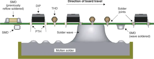
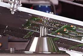
- Wave Soldering
Printed Circuit Board wave soldering, also known as through-hole soldering, is a common technique used in the assembly of electronic components to printed circuit boards. It is primarily used for through-hole components, such as connectors, switches or high power components which have leads that pass through holes on the PCB and require electrical connections on both sides of the board.
The wave soldering process typically involves the following steps:
- Flux application: A flux, typically in liquid or gel form, is applied to the PCB. The flux helps to remove any oxides and contaminants from the leads and pads, ensuring good solder wetting and bonding.
- Preheating: The PCB is preheated to a specific temperature to reduce thermal shock when it comes in contact with the molten solder wave.
- Wave soldering: The PCB is transported over a wave soldering machine. The machine contains a reservoir of molten solder, usually a lead-based alloy with a low melting point. A pump generates a wave of molten solder, which is shaped by a weir or a baffle to create a controlled flow or wave. The bottom side of the Printed Circuit Board with the through-hole components is brought into contact with the wave of molten solder. The solder wave wets the exposed leads and pads, forming a solder joint through a combination of heat and capillary action.
- Cooling: Once the solder joint is formed, the PCB moves away from the solder wave, and the solder solidifies as it cools. Some wave soldering machines have additional cooling zones or fans to expedite the cooling process.
- Inspection: The soldered PCBs undergo visual inspection and, in some cases, automated inspection techniques to detect any defects such as solder bridging, insufficient solder, or cold solder joints.
Wave soldering offers several advantages for through-hole component assembly:
- Efficiency: It is a high-speed soldering process that can handle a large number of PCBs in a relatively short time.
- Cost-effective: Wave soldering is a cost-effective method, especially for high-volume production, as it eliminates the need for manual soldering of each component.
- Reliable connections: The wave soldering process ensures reliable electrical connections between the through-hole components and the PCB, as the molten solder fully surrounds the leads and fills the holes.
- Selective Wave Soldering
Selective Wave soldering is a process that does not utilize the wave solder on the entire bottom side of the printed circuit assembly.
The areas to be selectively wave soldered can be defined utilizing wave solder pallets or wave solder fixtures to protect areas and components that are not to be exposed to the solder wave. These pallets are designed to hold and protect the components on a printed circuit assembly from the high temperatures and potential damage caused by the molten solder wave.
Wave solder pallets are typically made from a variety of materials, depending on the specific requirements. Common materials include fiberglass-reinforced epoxy composite (FR-4), polytetrafluoroethylene (PTFE), or other high-temperature resistant materials. The choice of material depends on factors such as the operating temperature, chemical resistance, and desired electrical properties.
Wave solder pallets are custom-designed to fit the specific PCB and assembly requirements. The pallets consist of a base, which holds the PCB, and a pattern of cavities, holes, or slots that accommodate the components to be soldered. The cavities and openings are precisely engineered to expose the desired soldering areas while protecting other areas of the PCB. The pallets may also have fiducial marks or alignment features to ensure accurate placement during assembly.
One of the primary functions of wave solder pallets is to manage heat transfer during the wave soldering process. They provide thermal insulation to prevent excessive heating of sensitive components and areas of the PCB. Pallets may include heat sinks, heat barriers, or venting features to optimize heat dissipation and maintain temperature uniformity across the PCB.
Wave solder pallets are designed to withstand the high temperatures and harsh conditions of the wave soldering process. They are typically durable, chemically resistant, and have a long service life. Pallets can be reused for multiple assembly runs, reducing costs and environmental impact.
- Selective Soldering
Selective Soldering is the process of pumping molten solder up through nozzles so that the solder will contact the bottom side of the printed circuit board and specific component leads at targeted areas forming solder joint connections on the component leads. The excess solder will flow back down the sides of the nozzle to the solder pot. The component leads are typically soldered by programming a series of positional steps allowing the leads to be soldered sequentially. This process offers advantages over full wave soldering in that it will allow access to small areas that may be difficult to reach or connections that may be “shadowed” by larger or taller components in a full wave solder process.
Inspection and Testing:
Once the soldering is complete, the assembled printed circuits undergo inspection and testing to ensure the quality and functionality of the assembly. Methods of inspection and testing Inspection of the Printed Circuit Assembly may include:
- Automated Optical Inspection (AOI): AOI systems use cameras and image processing algorithms to detect defects such as component misalignment, missing components, incorrect polarity, solder joint issues, and solder bridging.
- X-ray Inspection: X-ray systems are employed to inspect hidden or internal features of PCBs, such as solder joints under ball grid arrays (BGAs) and other surface-mount devices. X-ray inspection can identify defects like insufficient soldering, voids, and shorts.
- In-Circuit Testing (ICT): ICT involves the use of specialized test probes to check the electrical characteristics of individual components and verify the proper functioning of the PCB. It can identify issues like open circuits, short circuits, incorrect values, and faulty components.
- Functional Testing: This type of testing evaluates the overall performance and functionality of the assembled PCB, ensuring that it meets the desired specifications and requirements.
Automated inspection and testing offers several advantages over manual inspection methods, including:
- Improved Speed and Efficiency: AOI systems can inspect PCBs at high speeds, significantly reducing the time required for inspection compared to manual methods.
- Enhanced Accuracy and Consistency: Automated inspection minimizes human error and provides consistent results, ensuring that defects are reliably detected and categorized.
- Cost Savings: By automating the inspection process, AOI reduces the need for manual labor, leading to cost savings in terms of time, manpower, and potential rework or recalls caused by undetected defects.
- Increased Quality and Reliability: AOI helps identify defects early in the assembly process, allowing for prompt corrective actions and ensuring that only high-quality PCBs proceed to subsequent stages.
- Traceability and Documentation: Automated inspection systems as well as automated electrical and functional testing systems can generate detailed reports and documentation, providing a traceable record of the inspection and testing processes and facilitate analysis, troubleshooting, and quality control.
- Integration in Manufacturing Lines: AOI and testing systems can be integrated into printed circuit assembly manufacturing lines, typically positioned after the soldering process. They can be standalone machines or integrated within larger automated assembly systems, enabling seamless inspection without disrupting the overall production flow.
Depanelization:
Printed Circuits are often assembled in multiple up arrays or panels. The larger panels allow for smaller parts to run through the component assembly process in a more economical and time efficient manner. Multiple assemblies in a panel or array form also allow for additional tooling such as holes and fiducials that will be utilized by various machines in the assembly process.
The individual circuit assemblies need to be separated through the depanelization process. Depanelization can be carried out using various methods, depending on the complexity of the PCB design, the materials used, and the desired level of precision.
Depanelization techniques include:
- Manual Depanelization: This method involves using hand tools, such as shears, routers, or manual scoring systems, to cut or separate the boards from the panel. Manual depanelization is suitable for low-volume production or prototypes but can be time-consuming and less precise, and cause stress on components and electrically soldered joints.
- Guillotine Cutting: Guillotine cutters are used to cut through the panel and separate the individual PCBs. This method is quick and efficient, suitable for high-volume production. This depanelization method may not be suitable for PCBs with complex shapes or delicate components.
- V-Scoring: V-scoring involves creating a V-shaped groove on the top and bottom sides of the PCB panel, which defines the separation line between individual circuit assemblies. The boards can be separated by flexing them, causing the V-groove to break. V-scoring is commonly used when PCBs have straight-line separations and are relatively rigid.
- Tab Routing: In tab routing, small tabs or bridges are added between the PCBs and the panel to hold them in place during the manufacturing process. After assembly, the tabs are cut or broken to release the individual PCBs. Tab routing is suitable for PCBs with irregular shapes or sensitive components.
- Laser Cutting: Laser cutting is a precise and versatile method used for depanelization. A laser beam is used to cut through the panel along the predefined lines, separating the individual printed circuit assemblies. Laser cutting offers high accuracy, minimal stress on the boards, and is suitable for complex PCB designs.
Each depanelization method has its advantages and considerations depending on factors like production volume, PCB complexity, and budget. Manufacturers choose the most appropriate method based on their specific requirements and capabilities.
It’s important to note that depanelization requires careful handling to prevent damage to the PCBs and their components. Proper equipment, training, and quality control measures are essential to ensure the integrity and functionality of the separated PCBs.
Additional Processes
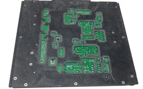
Depending on the specific requirements, additional processes may be involved, such as conformal coating, where a protective layer is applied to the PCB to safeguard it against environmental factors like moisture, dust, and temperature.
Summary
Printed circuit assembly is a critical stage in the production of electronic devices. It brings together the components necessary to create a fully functional circuit, and the quality of assembly plays a vital role in the overall performance and reliability of the final product.