The most common type of printed circuit board is the standard rigid PCB. This type of circuit board accounts for approximately 70% of the global printed circuit market. The basic purpose of a rigid circuit board is to provide a controlled, pre-manufactured, medium to connect individual pins of electronic components. The circuit board is created from individual materials (substrates, dielectrics and etched copper circuits) laminated together using copper plated holes to connect the electrical layers vertically. The number of etched copper layers can vary between one to over one hundred. Nearly every electronic product contains at least one printed circuit.
The etched circuits on the outermost layers are typically covered with a liquid photoimageable (LPI) soldermask leaving any solderable pads or plated through holes exposed. The main purpose of applying soldermask to the Printed Circuit Board is to protect the etched copper circuitry from corrosion and oxidation as well as prevent circuits from shorting during both the component assembly process and during operation of the Printed Circuit Board.
As optional ink may be silk screened over the soldermask and may include features such as component reference designators, polarity markings, part numbers, UL certifications and logos.
Several small printed circuit boards can be grouped together for processing as a panel or an array. This allows for multiple Printed Circuit Boards to be populated and assembled with electronic components simultaneously.
Recent advances in Printed Circuit Board manufacturing allow for a more streamlined and cost effective process and also allow for more complex and dense circuit designs to be manufacturable. These advances include using Direct Imaging capabilities for circuit etching as well as solder mask and ink application.
Prior to final inspection, packing and shipping, Rigid Printed Circuit Boards are typically electrical tested using a “bed of nails” or “flying probe tester” to ensure the boards do not contain shorted or open circuits.
Rigid printed circuit boards can be broken down to three basic categories based on the quantity of etched copper layers in the construction:
Single Sided Printed Circuit Boards
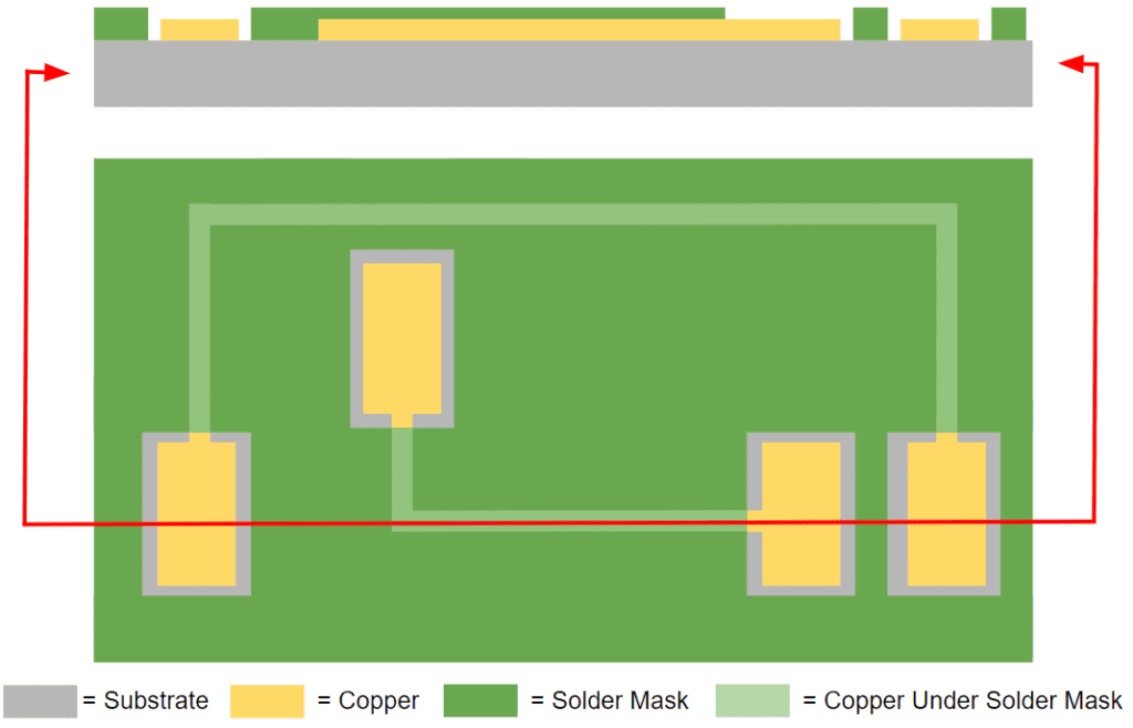
The simplest variation of a rigid printed circuit board, the single sided construction consists of a single etched circuit applied to a substrate, with the ares not to be connected to a component covered by a solder mask. Important note: If your circuit board includes plated through holes, even with etched circuitry on only one side, it is considered a double sided printed circuit board.
Double Sided Printed Circuit Boards
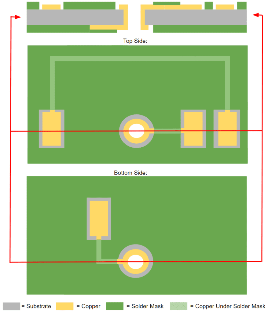
A double sided rigid printed Circuit Board utilizes drilled and copper plated holes to transfer the etched circuitry from the top side to the bottom side of the circuit board. The holes are mechanically drilled and plated with copper prior to the top and bottom circuits and pads being etched. The holes can be utilized to mount components with electrical leads (typically called Plated Through Holes), or can be used only to connect the top and bottom circuits (typically called vias).
Multilayer Printed Circuit Boards
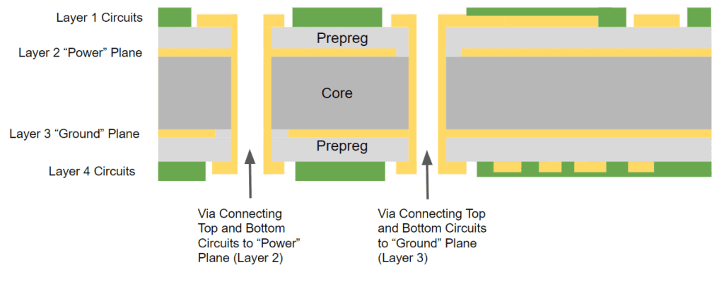
Multi Layer Rigid Printed Circuit Boards are created by laminating multiple substrates, dielectrics, and etched copper layers. The use of multiple layers allows for more complex and dense circuit routing and typically moves power and ground layers to etched circuitry or plane layers inside the printed circuit board. Due to the base materials used and lamination process, Multi Layer Printed Circuit Boards typically use an even number of layers such as 4, 6, 8, or more layers.
Printed Circuit Board Design
ECAD (electronic computer-aided design) software is typically used to design and create electronic structures which form the copper features in Rigid Printed Circuit Boards. ECAD tools such as Cadence, Mentor Graphics, and more are part of the electronic design cycle that may also include tools for schematic capture, logic simulation, signal integrity, thermal analysis and impedance calculation.
Data transfer from ECAD to your Printed Circuit Board supplier is typically in the form of individual copper layer and drill files in Gerber 274X format, or as a complete manufacturing file in the form of ODB++. A detailed fabrication drawing should be included that has all relevant information and specifications to manufacture the Rigid Printed Circuit Board. The fabrication drawing will also need to include information such as all relevant dimensions, hole sizes and quantities, material specifications, solder mask and silkscreen requirements, surface finish requirements and more.
Printed Circuit Board Material
There is a wide range of material choices for Rigid Printed Circuit Boards. The correct material choice will be dependent on meeting requirements such as temperature (both operating temperature and temperatures encountered during the component assembly processes), dielectric constant properties for impedance control, and thermal expansion requirements.
FR4 is the most common material for Rigid Printed Circuit Boards. FR4 is a class of printed circuit board base material made from a flame retardant epoxy resin and woven glass fabric composite. FR stands for flame retardant and FR4 meets the requirements of UL94V-0. FR4 has good adhesion to copper foil and has minimal water absorption, making it very suitable for standard Rigid printed Circuit Boards. This material comes in a wide variety of Tg (glass transition temperature), Td (thermal decomposition temperature) CTE (Coefficient of Thermal Expansion), and other properties. The choice of leaded or lead-free component assembly will have a large factor on the material properties required.
Other, less common, materials available include organic substrates composed of multiple paper layers impregnated with phenolic resin as well as non-woven or glass cloth layers impregnated with epoxy resin, polyimide, cyanate ester, BT resin, and others.
Inorganic substrates mainly include ceramic and metal materials, such as aluminum. The purpose of these substrates usually depends on heat dissipation requirements.
Capabilities
Capabilities when manufacturing Rigid Printed Circuit Boards vary greatly and are dependent on many factors including equipment, process and geographical location. Lead times, maximum layer counts, minimum copper feature size, smallest hole sizes and more are topics that can be discussed with your Rigid Printed Circuit Supplier’s Sales and Engineering teams. Early engagement with your supplier during the design cycle can help ensure your products are manufacturable and eliminate excess costs associated with incorrect material specifications and unnecessary manufacturing processes.